CHARACTERISTICS
- CMP (Chemical Mecanical Polishing), chemical mechanical polishing: While slicing the Slurry with the wafer in contact with the polishing PAD surface, chemically reacting the Wafer surface and moving the Head and Polishing Table relative to each other Technique for mechanically flattening the uneven part of Wafer
- Materials in direct contact with Wafer, generally use Polyurethane.
- CMP (Chemical Mechanical Polishing) is one of the eight major semiconductor manufacturing processes. It is a planarization technology that utilizes both chemical and mechanical principles to achieve a highly flat wafer surface.
In the CMP process, the wafer is pressed against the surface of a polishing pad under controlled pressure. Slurry is supplied to the interface between the wafer and the pad, enabling a chemical reaction on the wafer surface.
Simultaneously, abrasive particles contained in the slurry, together with the relative motion between the polishing head and the platen, mechanically remove surface materials and step height differences, resulting in wafer planarization.
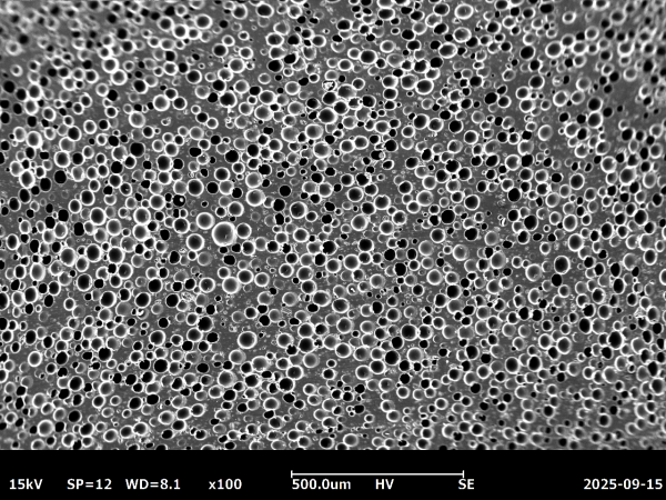
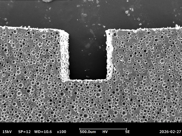
A critical consumable material used in this process is the CMP pad.
- The CMP pad is a product that directly contacts the wafer surface during the polishing process. It is typically manufactured by molding and curing polyurethane materials.
Point of Control
• Polymer Chemistry
- Hardness
- Abrasion Resistance
- Glass temperature
- Density
- Compression ratio
• Pad pore sizes and density
- Porefiller material type
- Porefiller density
- Porefiller size
- Porefiller distribution
Product Line-up